

High-power LED packaging technology
Nov.20.2024
High-power LED packaging has been a research hotspot in recent years due to its complex structure and process, and directly affects the performance and life of LED. In particular, high-power white light LED packaging is a hotspot among research hotspots.
The functions of LED packaging mainly include: 1. Mechanical protection to improve reliability; 2. Strengthen heat dissipation to reduce chip junction temperature and improve LED performance; 3. Optical control to improve light output efficiency and optimize beam distribution; 4. Power supply management, including AC/DC conversion and power supply control.
The selection of LED packaging methods, materials, structures and processes is mainly determined by factors such as chip structure, optoelectronic/mechanical properties, specific applications and costs. After more than 40 years of development, LED packaging has gone through the development stages of bracket type (Lamp LED), SMD type (SMD LED), bare core type LED (COB LED).
Key technologies of high-power LED packaging
High-power LED packaging mainly involves light, heat, electricity, structure and process. These factors are both independent of each other and affect each other. Among them, light is the purpose of LED packaging, heat is the key, electricity, structure and process are means, and performance is the specific embodiment of the packaging level. From the perspective of process compatibility and reducing production costs, LED package design should be carried out simultaneously with chip design, that is, the package structure and process should be considered when designing the chip. Otherwise, after the chip is manufactured, the chip structure may be adjusted due to the need for packaging, thereby extending the product development cycle and process cost, and sometimes even impossible.
01 Low thermal resistance packaging process For the current LED light efficiency level, since about 80% of the input electrical energy is converted into heat, and the LED chip area is small, chip heat dissipation is a key issue that must be solved in LED packaging. It mainly includes chip layout, packaging material selection (substrate material, thermal interface material) and process, heat sink design, etc.
02 High light extraction rate packaging structure and process During the use of LEDs, the loss of photons generated by radiation recombination when emitted outward mainly includes three aspects: internal structural defects of the chip and absorption of the material; reflection loss of photons at the exit interface due to the refractive index difference; and total reflection loss caused by the incident angle being greater than the critical angle of total reflection. Therefore, many rays cannot be emitted from the chip to the outside. By coating a layer of transparent glue (potting glue) with a relatively high refractive index on the surface of the chip, since the glue layer is between the chip and the air, the loss of photons at the interface is effectively reduced, and the light extraction efficiency is improved. In addition, the role of potting glue also includes mechanical protection of the chip, stress release, and as a light-guiding structure. Therefore, it is required to have high light transmittance, high refractive index, good thermal stability, good fluidity, and easy spraying. In order to improve the reliability of LED packaging, the potting glue is also required to have low hygroscopicity, low stress, and aging resistance. Currently commonly used potting glues include epoxy resin and silicone. Silicone is significantly better than epoxy resin because of its high light transmittance, high refractive index, good thermal stability, low stress, and low hygroscopicity. It is widely used in high-power LED packaging, but the cost is relatively high.
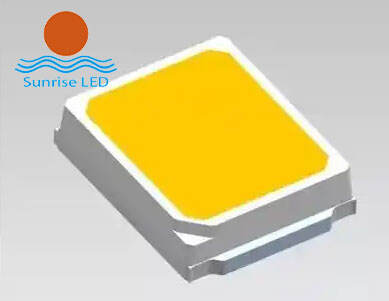
In recent years, LED chips have gradually become the darling of the display industry. With the advantages of high brightness, self-luminescence, and full color, they have continuously entered various display venues, and SMD packaging and COB packaging are the main factors driving this development.
Surface mount three-in-one (SMD) LED emerged in 2002 and gradually occupied the market share of LED display devices, shifting from pin-type packaging to SMD. Surface mount packaging is to bond a single or multiple LED chips to a metal bracket with a plastic "cup-shaped" outer frame (the outer pins of the bracket are connected to the P and N poles of the LED chip respectively), and then fill the plastic outer frame with liquid packaging glue, and then bake it at high temperature to form it, and finally cut it into individual surface mount packaged devices. Because surface mount technology (SMT) can be used, the degree of automation is relatively high. Compared with pin-type packaging technology, SMD LEDs have good performance in brightness, consistency, reliability, viewing angle, appearance, etc.